Board Insertion
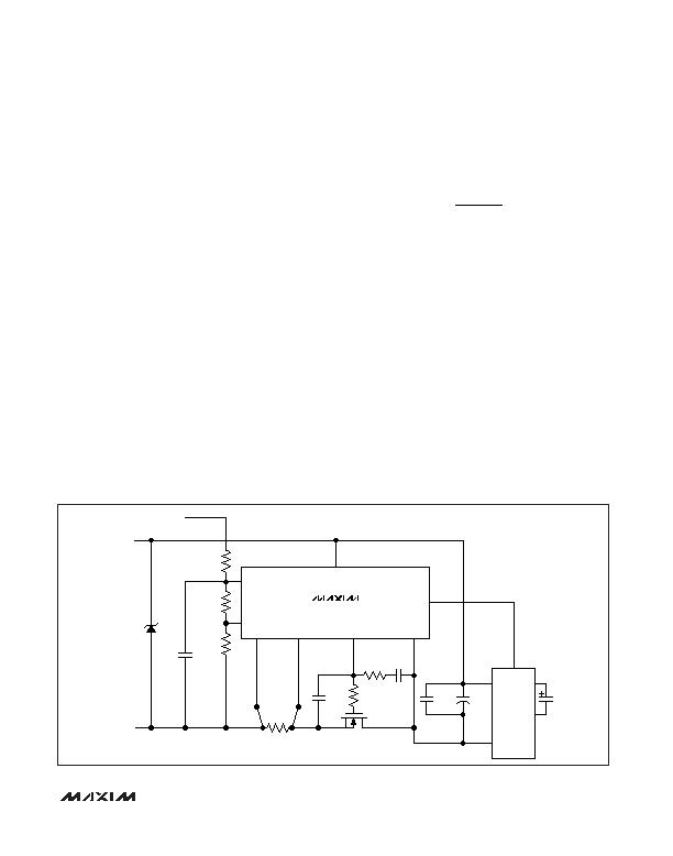
Figure 7a shows a typical hot-swap circuit for -48V sys-
tems. When the circuit board first makes contact with
the backplane, the DRAIN to GATE capacitance (C
gd
)
of Q1 pulls up the GATE voltage to roughly IV
EE
x C
gd
/
(C
gd
+ C
gs
)I. The MAX5949_ features an internal
dynamic clamp between GATE and V
EE
to keep the
gate-to-source voltage of Q1 low during hot insertion,
preventing Q1 from passing an uncontrolled current to
the load. For most applications, the internal dynamic
clamp between GATE and V
EE
of the MAX5949A/
MAX5949B eliminates the need for an external gate-to-
source capacitor C1. Resistor R3 limits the current into
the clamp circuitry during card insertion.
Power-Supply Ramping
The MAX5949_ can reside either on the backplane or
the removable circuit board (Figure 7a). Power is deliv-
ered to the load by placing an external n-channel
MOSFET pass transistor in the power-supply path.
After the circuit board is inserted into the backplane
and the supply voltage at V
EE
is stable and within the
undervoltage and overvoltage tolerance, the MAX5949_
turn on Q1. The MAX5949_ gradually turn on the exter-
nal MOSFET by charging the gate of Q1 with a 45礎
current source.
Capacitor C2 provides a feedback signal to accurately
limit the inrush current. The value of C
2
can be
calculated:
where C
L
is the total load capacitance, C3 + C4, and
I
PU
is the MAX5949_ gate pullup current.
Figure 7b shows the inrush current waveform. The cur-
rent through C2 controls the GATE voltage. At the end
of the DRAIN ramp, the GATE voltage is charged to its
final value. The GATE-to-SENSE clamp limits the maxi-
mum V
GS
to about 18V under any condition.
Board Removal
If the card is removed from a live backplane, the output
capacitor on the card may not be immediately dis-
charged. While the output capacitor is discharging, the
MAX5949_ continues to operate as if the input supply
were still connected because the output capacitor tem-
porarily supplies operating current to the IC. If the cir-
cuit is connected as in Figure 7a, the voltage at the UV
pin falls below the V
UVL
, and the MAX5949_ turns off
the external MOSFET. If R4 in the circuit is connected
directly to the -48V return, the external MOSFET
remains on until the capacitor is discharged sufficiently
to drop the UV pin voltage to V
UVL
.
C
I x C
I
PU
L
INRUSH
2
=
-48V Hot-Swap Controllers
with External R
SENSE
_______________________________________________________________________________________ 9
V
EE
SENSE
GATE
DRAIN
V
DD
OV
UV
PWRGD
MAX5949B
-48V RTN
-48V
R4
549k&
1%
R5
6.49k&
1%
R6
10k&
1%
R1
0.02&
5%
R3
1k&
5%
R2
10&
5%
C1**
470nF
25V
Q1
IRF530
C2
15nF
100V
GATE IN
VICOR
VI-J3D-CY
V
IN+
V
IN-
C4
100礔
100V
C3
0.1礔
100V
C5
100礔
10V
*
10nF
-48V RTN
(SHORT PIN)
*DIODES INC. SMAT70A.
**OPTIONAL.
Figure 7a. Inrush Control Circuitry
发布紧急采购,3分钟左右您将得到回复。
相关PDF资料
MAX5950ETJ+
IC PWM CTRL HOT-SW 12V 32TQFN-EP
MAX5952CUAX+
IC PSE CNTRLR FOR POE 36-SSOP
MAX5953DUTM+
IC INTERFACE 802.3AF 48TQFN
MAX5954LETX+T
IC PCI EXP/HOT-PLUG CTRLR 36TQFN
MAX5955BEEE+
IC DUAL HOT-SWAP CTRLR 16-QSOP
MAX5957AETN+T
IC TRPL PCI EXP/HOT-PLUG 56-TQFN
MAX5960AECS+T
IC CTRLR HOT-PLUG QD 80-TQFP
MAX5963UTL+T
IC HOT SWAP DIO ORING CTL 40TQFN
相关代理商/技术参数
MAX5949BESA-T
功能描述:热插拔功率分布 RoHS:否 制造商:Texas Instruments 产品:Controllers & Switches 电流限制: 电源电压-最大:7 V 电源电压-最小:- 0.3 V 工作温度范围: 功率耗散: 安装风格:SMD/SMT 封装 / 箱体:MSOP-8 封装:Tube
MAX5950ETJ
功能描述:电压模式 PWM 控制器 RoHS:否 制造商:Texas Instruments 输出端数量:1 拓扑结构:Buck 输出电压:34 V 输出电流: 开关频率: 工作电源电压:4.5 V to 5.5 V 电源电流:600 uA 最大工作温度:+ 125 C 最小工作温度:- 40 C 封装 / 箱体:WSON-8 封装:Reel
MAX5950ETJ+
功能描述:电压模式 PWM 控制器 12V PWM Controller w/Hot-Swap RoHS:否 制造商:Texas Instruments 输出端数量:1 拓扑结构:Buck 输出电压:34 V 输出电流: 开关频率: 工作电源电压:4.5 V to 5.5 V 电源电流:600 uA 最大工作温度:+ 125 C 最小工作温度:- 40 C 封装 / 箱体:WSON-8 封装:Reel
MAX5950ETJ+T
功能描述:电压模式 PWM 控制器 12V PWM Controller w/Hot-Swap RoHS:否 制造商:Texas Instruments 输出端数量:1 拓扑结构:Buck 输出电压:34 V 输出电流: 开关频率: 工作电源电压:4.5 V to 5.5 V 电源电流:600 uA 最大工作温度:+ 125 C 最小工作温度:- 40 C 封装 / 箱体:WSON-8 封装:Reel
MAX5950ETJ-T
功能描述:电压模式 PWM 控制器 RoHS:否 制造商:Texas Instruments 输出端数量:1 拓扑结构:Buck 输出电压:34 V 输出电流: 开关频率: 工作电源电压:4.5 V to 5.5 V 电源电流:600 uA 最大工作温度:+ 125 C 最小工作温度:- 40 C 封装 / 箱体:WSON-8 封装:Reel
MAX5950EVKIT
制造商:Maxim Integrated Products 功能描述:12V PWM CONTROLLER WITH HOT-SWAP - Rail/Tube
MAX5951ETJ
功能描述:电压模式 PWM 控制器 RoHS:否 制造商:Texas Instruments 输出端数量:1 拓扑结构:Buck 输出电压:34 V 输出电流: 开关频率: 工作电源电压:4.5 V to 5.5 V 电源电流:600 uA 最大工作温度:+ 125 C 最小工作温度:- 40 C 封装 / 箱体:WSON-8 封装:Reel
MAX5951ETJ+
功能描述:电压模式 PWM 控制器 12V/5V Buck PWM Controller RoHS:否 制造商:Texas Instruments 输出端数量:1 拓扑结构:Buck 输出电压:34 V 输出电流: 开关频率: 工作电源电压:4.5 V to 5.5 V 电源电流:600 uA 最大工作温度:+ 125 C 最小工作温度:- 40 C 封装 / 箱体:WSON-8 封装:Reel
